Showing posts with label to. Show all posts

Thursday, July 11, 2013

230 V AC To 400 V DC Power Supply Circuit Diagram


Description

               A lot of students are who dont know how to convert 230 volt AC to 400 DC. So today I am published   230 V AC to 400 V DC circuit diagram on my blog. Working principle of this circuit diagram is very simple. You already knew the working principle of a bridge rectifier. This circuit is same as bridge rectifier and the working principle is also same. The fuse is used to protect the circuit, if the current is greater than 1 A.


Parts List

Component No:Value
F11 A
B1IN4007 
C1470MF/450V 
V1230 V AC 


Source by : link
{ Read More }


Wednesday, July 10, 2013

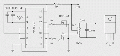
DC to AC Inverter with IC CD4047

This DC to AC inverter circuit work based on unstable multi vibrator does. In this circuit, IC CD4047 is chosen as a heart of unstable multivibrator, because this IC type gives a complementary output that has opposite phase to another ( pin 10 and 11 as seen in Figure 1), and has 50 % duty cycle that satisfy to generate a pulse for inverter.

DC to AC Inverter with IC CD4047 Circuit Diagram

DC to AC Inverter Circuit Diagram

{ Read More }


Use A DAC To Bias Your Varactor Diode

Varactor (or “varicap”) diodes are used primarily in radio-frequency (RF) circuits to provide a capacitance that can be varied by changing the applied voltage. These types of diodes often are used for tuning circuits, such as RF oscillators and filters found in wireless applications like wireless microphones and radios. Designers, then, should know about the benefits of using a nonvolatile digital-to-analog converter (DAC) to provide the biasing voltage of a varactor diode used as a voltage-controlled capacitor.

The varactor diode is operated under reverse bias, which creates a depletion zone around the P-N junction. Changing the level of the reverse bias changes the thickness of the depletion region and, thus, the effective capacitance of the diode. Increasing voltage causes a decrease in capacitance.

Varactor diodes are specified with a nominal capacitance value and the range of capacitance that can be achieved with a maximum and minimum voltage level. Increasing the bias voltage range increases the capacitance range available, but designers can also look for varactors with a larger capacitance- to-voltage ratio.

A convenient solution for creating a varying bias voltage is to use a DAC. Most DACs have an output voltage range of 0 V to +5.5 V. If a higher voltage bias is required, though, then a high-voltage DAC can be used. However, it may be more cost-effective to use a low-cost, high-voltage operational amplifier in a non-inverting configuration to provide level shifting of the output voltage from a common 5.5-V DAC.

 
The LC-tank circuit portion of a voltage-controlled oscillator allows for FM modulation in wireless microphones and radios. Its back-to-back varactor configuration minimizes the effects of RF modulation.

Using a DAC does introduce sources of potential error. The varactor is affected by any form of amplitude variation of the bias voltage, resulting in an undesired shift in capacitance. Deterministic errors can be accounted for when using the microcontroller to program the DAC output voltage. The primary sources of error that should be considered include varactor nonlinearity, offset errors, and DAC integral nonlinearity (INL). RF modulation may also be caused by voltage induced from a noise source – perhaps from an antenna in the system. The figure shows an LC-tank circuit portion of a voltage-controlled oscillator. This circuit allows for FM modulation in the aforementioned wireless microphone or radio.

Here, a back-to-back varactor configuration minimizes the effects of RF modulation. If a varying signal is injected, the bias across one diode increases as the other decreases, keeping overall capacitance unchanged. Note that the two diodes are in series with each other, so capacitance is half of a single varactor setup.

To also prevent RF signals from affecting the circuitry outside the tuning circuit, the bias voltage is fed through an isolation resistor or an RF choke. There are other benefits to using a DAC to bias a varactor diode. For example, multiple-output-channel DAC devices can be used in a multistage application. Additionally, in a four-channel DAC, three channels could potentially be used for separate band-pass filters for low-, mid-, and high-frequency filtering. The fourth output could be used for offset voltage calibration elsewhere in the circuit, or it could be turned off when it isn’t in use. Space and design time can be saved by avoiding having to set up separate biasing schemes.

Some DACs, such as the MCP4728, also offer on-board nonvolatile memory, which can store configuration data such as output-voltage levels and channel status (on/off). This enables the device to be reset or powered up into a known set state, which could allow a pre-programmed tune to be stored. The tune could be recalled when a desired event or input occurs or when power is lost and restored.
{ Read More }


Thursday, July 4, 2013

4 Bit Analogue to Digital Converter

The operation of the converter is based on the weighted adding and transferring of the analogue input levels and the digital output levels. It consists of comparators and resistors. In theory, the number of bits is unlimited, but each bit needs a comparator and several coupling resistors. The diagram shows a 4-bit version. The value of the resistors must meet the following criteria:
  • R1:R2 = 1:2;
  • R3:R4:R5 = 1:2:4;
  • R6:R7:R8:R9 = 1:2:4:8.
The linearity of the converter depends on the degree of precision of the value of the resistors with respect to the resolution of the converter, and on the accuracy of the threshold voltage of the comparators. This threshold level must be equal, or nearly so, to half the supply voltage. Moreover, the comparators must have as low an output resistance as possible and as high an input resistance with respect to the load resistors as feasible. Any deviation from these requirements affects the linearity of the converter adversely.
Circuit diagram:
4-bit_AnalogueTo_Digital_Converter-Circuit-Diagramw
4-Bit Analogue to Digital Converter Circuit Diagram

If the value of the resistors is not too low, the use of inverters with an FET (field-effect transistor) input leads to a near-ideal situation. In the present converter, complementary metal-oxide semiconductor (CMOS) inverters are used, which, in spite of their low gain, give a reasonably good performance. If standard comparators are used, take into account the output voltage range and make sure that the potential at their non-inverting inputs is set to half the supply voltage. If high accuracy is a must, comparators Type TLC3074 or similar should be used. This type has a totem-pole output. The non-inverting inputs should be interlinked and connected to the tap of a a divider consisting of two 10 kΩ resistors across the supply lines. It is essential that the converter is driven by a low-resistance source. If necessary, this can be arranged via a suitable op amp input buffer. The converter draws a current not exceeding 5 mA.
 
 
Source :www.ecircuitslab.com
{ Read More }


Monday, May 27, 2013

How to Use IC 741 as a Comparator

Weve been using this IC probably since we were kids, I am referring to this wonderful little IC 741, through which virtually any circuit designing becomes feasible. It almost alone is able to handle many complex functions and makes circuit configuration very easy, thats why its one of the favorite chips not only with the new electronic hobbyists but also with the experienced engineers.
Here we are discussing one of the simple application circuits of this IC where it is being configured as a comparator, no surprise the following applications can be modified in numerous different ways as per the user preference.
As the name suggests, comparator means the function of comparing between a particular set of parameters or may be just a couple of magnitudes as in the case.

Since in electronics we are primarily dealing with voltages and currents, these factors become the sole agents and are used for operating or regulating or controlling the various components involved.

In the proposed design, where the IC 741 is being used as a comparator, basically different voltage levels are used as the referring and comparaing parameters by the IC.

The two input pins named the inverting (with a minus sign)and the non-inverting pin (with a + sign) become the sensing inputs of the IC 741.

When used as a comparator, one of the pins out of the two is applied with a fixed reference voltage while the other pin is fed with the voltage whose level needs to be monitored.

The monitoring of the above voltage is done with reference to the fixed voltage thats been applied to the other complementary pin.

Therefore if the voltage which is to be monitored goes above or falls below the fixed reference threshold voltage, the output reverts state or changes its original condition or changes its output voltage polarity.

Letsanalyze the above explanation by studying the following example circuit of a light sensor switch.

Looking at the circuit diagram we find the circuit configured in the following way:

The IC 741 is at the center.

Its Pin #7 which is the +supply pin is connected to the positive rail, similarly its pin #4 which is the negative supply pin is connected to the negative or rather the zero supply rail of the power supply.

The above couple of pin connections powers the IC so that it can carry on with its intended functions.

Now as discussed earlier, pin #2 of the IC is connected at the junction of two resistors whose ends are connected to the power supply positive and negative rails. This arrangement of the resistors is called a potential divider, meaning the potential or the voltage level at the junction of these resistors will be approximately the half of the supply voltage, so if the supply voltage is 12, the junction of the potential divider network will be 6 volts and so on.

If the supply voltage is well regulated, the above voltage level will also be well fixed and therefore can be used as the reference voltage for the pin #2.

So if we take 6 as the junction voltage of the resistors, this voltage becomes the reference voltage at pin #2 which means the IC will monitor and respond to any voltage that might go above this level.

The sensing voltage which is to be monitored is applied to pin #3 of the IC, in our example it is via an LDR. The pin #3 is connected at the junction of the LDR pin and a preset terminal.
That means this junction again becomes a potential divider, whose voltage level this time is not fixed because the LDR value cannot be fixed and will vary with the ambient light conditions.
Now suppose you want the circuit to sense the LDR value at some point just around when dusk falls, you adjust the preset such that the voltage at pin #3 or at the junction of the LDR and the preset just crosses above the 6 volt mark.

When this happens the value rises above the fixed reference at pin #2, this informs the IC about the sense voltage rising above the refefnce voltage at pin #2, this instantly reverts the output of the IC which changes to positive from its initial zero voltage position.

The above change in the state of the IC from zero to positive, triggers the relay driver stage which switches ON the load or the lights which might be connected to the relevant contacts of the relay.

Mind you, the values of the resistors connected to pin #2 may also be altered for altering the sensing threshold of pin #3, so they are all inter-depended, giving you a wide angle of variation of the circuit parameters.

Another feature of the R1 and R2 is that it avoids the need of using a dual polarity power supply making the involved configuration very simple and neat.

As shown below, the above explained operation response can be just reversed by interchanging the input pin positions of the IC or, by considering another option where we only inter-change the positions of the LDR and the preset.



{ Read More }


Sunday, May 19, 2013

Nokia 3510i Convert to Nokia 3595

Nokia 3510i Convert to Nokia 3595 Follow the Instruction.
{ Read More }


Friday, May 17, 2013

How to Increase Current 7805 Voltage Regulator

7805 voltage regulator is one variant of the three terminal Positive Voltage Regulator. IC 7805 operated at maximum load current at a positive fixed voltage 5V 1A, but work on the maximum current will increase the thermal level. Aluminum heatsink is needed to reduce the level of heat, though internally IC 7805 has a thermal over-load protection.

The voltage regulator that works at the maximum rate is an unfavorable condition. Besides the heat level increases, it will likely be fatal if an increase in the load current due to short circuit. A good idea is to increase load current capability by adding an external transistor.

Based on the manual of IC 7805 has given a basic circuit to operate the IC at higher load currents. Download 7805 datasheet manual.

7805 Voltage Regulator Circuit 


In the following circuit to increase 7805 output current up to 3 amperes, must be added a complementary NPN transistor MJ2955. The advantage of this technique is to overcome when there is short-circuit as described above. When there is a voltage drop, then the circuit will reduce the maximum current consumption. So the problem can be solved.

7805 Voltage Regulator Circuit

Transistor BD240C in the DC voltage regulator circuit serves as a current limiting. The transistor is open when the voltage at 10R+0.22R be higher than 0.6-0.7 Volts, which leads to a reduction to zero of the T2 base current. The voltage at which the short-circuit protection starts to act, is given by voltage sum on 0.22R and 10R. Base voltage is determined by resistors 10R and 150R. In this circuit did not happen over-thermal when short-circuit occured, the maximum current was only 0.5 Ampere.

Hope this simple explanation may help in making a higher current-voltage regulator using IC 7805. You can open the manual datasheet of the 7805 voltage regulator for more information.
{ Read More }


Tuesday, May 14, 2013

1 25V to 25V To DC power supply


This is a DC power supply circuit.This circuit is based on LM317 Variable Regulator.This Regulator needs at least 28v(DC).Then it will out put 1.25v to 25v DC.So I suppose this would be an important circuit for you all.# 5K ohm Change If you want to change the out put voltage
# This circuit supplies 1.3A.

{ Read More }


Wednesday, May 8, 2013

Beeper to find short circuits

This circuit uses two 741s or equivalent op amp to form a beeper that is used to detect short circuits.
This design offers a way to trace resistance in the milliohm range, right to a short between bridged traces beneath a solder mask. A1 is configured as a multivibrator. R1 and C1 determine the frequency of oscillation and Q1 and Q2 boost the output. Assuming a virtual ground at the output of A2, free-run frequency is about 1kHz. Q1 and Q2 deliver a +/-10v squarewave to R4, dumping a +/-100mA through a short circuit placed across the probe tips.

R5 ensures that the open circuit voltage never exceeds +/-0.1v. A2 monitors the voltage between the probes. When the probes are open, A2s gain equals the R4/R5 divider loss, and the output of both amplifiers is identical. This has two effects: First, hysteresis is greatly increased and frequency falls to a low growl, and secondly, the loudspeaker that bridges the two in-phase outputs is effectively silenced. A dead short across the probe tips will return nothing to A2 and the circuit will squeal at its nominal 1kHz rate. Anything less than a perfect short produces some output from A2, increasing multivibrator hysteresis and lowering the pitch.
{ Read More }


Wednesday, May 1, 2013

How to build Personal alarm

Small, portable, anti-bag-snatching unit
Also suitable for doors and windows control

Circuit diagram

  • R1 330K 1/4W Resistor
  • R2 100R 1/4W Resistor
  • C1 10nF 63V Polyester or Ceramic Capacitor
  • C2 100µF 25V Electrolytic Capacitor
  • Q1 BC547 45V 100mA NPN Transistor
  • Q2 BC327 45V 800mA PNP Transistor
  • SW1 Reed Switch and small magnet (See Notes)
  • SPKR 8 Ohm Loudspeaker (See Notes)
  • B1 3V Battery (two A or AA cells wired in series etc.)

Device purpose:

This circuit, enclosed in a small plastic box, can be placed into a bag or handbag. A small magnet is placed close to the reed switch and connected to the hand or the clothes of the person carrying the bag by means of a tiny cord. If the bag is snatched abruptly, the magnet looses its contact with the reed switch, SW1 opens, the circuit starts oscillating and the loudspeaker emits a loud alarm sound. The device can be reverse connected, i.e. the box can be placed in a pocket and the cord connected to the bag. This device can be very useful in signalling the opening of a door or window: place the box on the frame and the magnet on the movable part in a way that magnet and reed switch are very close when the door or window is closed.

Circuit operation:

A complementary transistor-pair is wired as a high efficiency oscillator, directly driving a small loudspeaker. Low part-count and 3V battery supply enable a very compact construction.

Notes:

  • The loudspeaker can be any type, its dimensions are limited only by the box that will contain it.
  • An on-off switch is unnecessary because the stand-by current drawing is less than 20µA.
  • Current consumption when the alarm is sounding is about 100mA.
  • If the circuit is used as anti-bag-snatching, SW1 can be replaced by a 3.5mm mono Jack socket and the magnet by a 3.5mm. mono Jack plug with its internal leads shorted. The Jack plug will be connected with the tiny cord etc.
  • Do not supply this circuit with voltages exceeding 4.5V: it will not work and Q2 could be damaged. In any case a 3V supply is the best compromise
{ Read More }


Friday, March 29, 2013

Speaker to microphone converter circuit


This circuit is a simple approach for converting a loud speaker into a microphone. When the sound waves fall on the diaphragm of a speaker, there will be fluctuations in the coil and there will be a small proportional induced voltage. Usually this induced voltage is very low in magnitude and useless. Here in the circuit the low voltage is amplified using transistors to produce a reasonable output. The transistor Q1 is wired in common base mode and produces the required voltage gain. The transistor Q2 is wired as an emitter follower to produce enough current gain. The voice quality of this circuit will not be as much as a conventional microphone but quite reasonable quality can be obtained. To set up the circuit, keep the preset R2 at around 10 Ohms and connect the battery. Now adjust R2 to obtain the optimum sound quality.


Notes.

* Assemble the circuit on a general purpose PCB. * Power the circuit from a 9 V PP3 battery. * A 3 inch speaker can be used as K1. * All capacitors must be rated at least 15V. * An 8 Ohm speaker or head phone can be connected at the output to hear the picked sound.
{ Read More }


IconIconIconFollow Me on Pinterest