Showing posts with label amplifier. Show all posts

Friday, January 10, 2014

High Voltage 3 Watt Audio Power Amplifier

The LM4954 is an audio power amplifier primarily designed for demanding applications in mobile phones and other portable communication device applications. It is capable of delivering 2.4 Watts of continuous average power to an 8 BTL load with less than 1% THD+N from a 7VDC power supply. Boomer audio power amplifiers are designed specifically to provide high quality output power with a minimal number of external components. The LM4954 does not require output coupling capacitors or bootstrap capacitors, and therefore is ideally suited for lower-power portable applications where minimal space and power consumption are primary requirements.

High Voltage 3 Watt Audio Power Amplifier Circuit Diagram

High Voltage 3 Watt Audio Power Amplifier Circuit
The LM4954 features a low-power consumption global shutdown mode which is achieved by driving the shutdown pin with logic low. Additionally, the LM4954 features an internal thermal shutdown protection mechanism.
The LM4954 contains advanced pop & click circuitry which eliminates noises that would otherwise occur during turn-on and turn-off transitions.
The LM4954 is unity-gain stable and can be configured by external gain-setting resistors.

Key Specification:
Wide Power Supply Voltage Range 2.7 <= VDD <= 9V
Output Power: VDD = 7V, 1% THD+N 2.4W (typ)
Quiescent power supply current 3mA (typ)
PSRR: VDD = 5V and 3V at 217Hz 80dB (typ)
Shutdown power supply current 0.01µA (typ)

Features:
  • No output coupling capacitors, snubber networks or bootstrap capacitors required
  • Unity gain stable
  • Externally configurable gain
  • Ultra low current active low shutdown mode
  • BTL output can drive capacitive loads up to 100pF
  • "Click and pop" suppression circuitry
  • 2.7V - 9.0V operation
  • Available in space-saving microSMD package
  • Applications
  • Mobile Phones
  • PDAs
  • Source: http://www.ecircuitslab.com/2011/06/high-voltage-3-watt-audio-power.html


    { Read More }


    Saturday, July 13, 2013

    Bench Amplifier Based on LM386

    A small 325mW amplifier with a voltage gain of 200 that can be used as a bench amplifier, signal tracer or used to amplify the output from personal radios, etc.

     Circuit Diagram


    Notes:
    The circuit is based on the National Semiconductor LM386 amplifier. In the diagram above, the LM386 forms a complete non-inverting amplifier with voltage gain of x200.

    A datasheet in PDF format can be downloaded from the National Semiconductor. The IC is available in an 8 pin DIL package and several versions are available; the LM386N-1 which has 325mW output into an 8 ohm load, the Lm386N-3 which has 700mW output and the LM386N-4 which offers 1000mW output. all versions work in this circuit.

    The gain of the Lm386 can be controlled by the capacitor across pins 1 and 8. With the 10u cap shown above, voltage gain is 200, omitting this capacitor and the gain of the amplifier is 20.

    The IC works from 4 to 12Volts DC, 12Volt being the maximum recommended value. The internal input impedance of the amplifier is 50K, this is shunted with a 22k log potentiometer so input impedance in this circuit will be lower at about 15k. The input is DC coupled so care must be taken not to amplify any DC from the preceeding circuit, otherwise the loudspeaker may be damaged. A coupling capacitor may included in series with the 22k control to prevent this from happening.

    The Finished Circuit.

    { Read More }


    Thursday, July 11, 2013

    SW RF Pre Amplifier

    A radio frequency amplifier to boost SW reception. Frequency range approximately 5 to 20 MHz.

    SW RF Pre-Amplifier Circuit Diagram


    Notes:
    The problem with amplifying weak radio signals is that you also amplify the noise. What you can receive depends on how much background noise is present, whether it be man made interference or static. In this design the RF signal is first met by a resistive attenuator, this is necessary as strong signals could otherwise overload your receiver.

    The transformer T1 is would on a 1 inch diameter ferrite loop. The primary (antenna side) is 2 turns of 22 swg wire. The secondary is 4 turns of 22 swg wire. The 4 turns are spaced to occupy roughly half the coils circumference. The approximate inductance of the secondary is 20uH. To cover 5 to 20 Mhz a capacitor tuning from around 3pF to 200pF is required. A standard capacitor of 400 or 500pF (full mesh) can be used by including a series capacitor, C2 in the above Capacitors. Capacitors in series behave the same as resistors in parallel. The smallest capacitance is just less than the smallest capacitor in series and highest value also less than the highest capacitance. With a 220pF capacitor for C2 and a 500pF variable capacitor (that tunes down to 5pF) the effective capacitance tunes 143pF to about 4.8pF.

     This is roughly correct and not critical as the gain of the FET will amplify frequencies outside the tuned circuit range. The 2N3819 FET operates in common source. The series base resistor R1 is included to even out the response, the internal gate source impedance is thus increased by R1 at higher frequencies. The drain circuit includes a 2.5mH choke. A 4.7mH can also be used. As the Q factor of these coils are high, a series resistor R3 is introduced to flatten the response. The frequency response is shown below calculated at 10% increments of VC1:

    The output impedance from the FET is high, so is buffered by the BC108C in emitter follower mode. Current drain is around 3mA from a 9 Volt battery. As with any RF circuit, the circuit is sensitive to noise and interference. A metal or aluminum box would be a good choice for this project. However, on my trusty breadboard, this circuit preformed well, and weak signals were boosted well.

    Parts List:

    R1     100k
    R2     1k
    R3     330
    R4     47k
    R5     68k
    R6     4.7k
    VR1     4.7k

    C1     100n
    C2     220p
    C3     100n
    C4     1n
    C5     10n
    VC1         500pF

    L1     2.5m

    J1     2N3819
    Q1     BC108B
    { Read More }


    Wednesday, July 10, 2013

    LA4440 Stereo Amplifier Circuit Diagram

    LA4440 is a dual channel audio amplifier IC. It can be used in two modes; one is Stereo amplifier and another Bridge amplifier mode. The LA4440 is a monolithic linear IC from Sanyo. Here I give the both circuit mode of amplifier using IC LA4440.

    When the IC LA4440 is Stereo mode in the circuit, its output power is 6w+6w. In stereo mode use two pieces speaker of 2Ωto8Ω.

    LA4440 Stereo Amplifier Circuit Diagram

    C10 is filter capacitor used to reduce the ripple of supply voltage. Don’t decrease the value of capacitor C6&C7 less than 100uF, 10v, it may causes of the output at low frequencies goes lower. The pin-6 of LA4440 amplifier circuit  is audio input pin; it used in stereo amplifier mode but in bridge mode it is grounded. C8&C9 are polyester film capacitor used to preventing oscillation, and R1&R2 used for the same reason as filter resistor. Though the maximum supply voltage for both circuit of amplifier is 18V but we recommend to use a 12V,3A power supply. Use a good quality heat sink with LA4440.

    I think here you see little comparison between stereo and bridge amplifier of LA4440. If you want to make this amplifier project, then I recommend you the bridge one. I think it is ideal for a beginner. And I love its wattage rather than Stereo mode. There is also a possibilities as I say, make two copies of circuit of bridge amplifier for stereo, it will give you 19w+19w of audio power output.
    { Read More }


    Saturday, July 6, 2013

    10 10 W Stereo Amplifier with tda2004

    Hello! in this post I will show a small amplifier using integrated circuit TDA2004 get two outputs 10 watts, the circuit is very simple, if you want to change the circuit, or a mono version refer to the datasheet tda2004!
    The circuit is powered by source between 12 and 15 volts with a current of 1.5 Amperes.
     
    See the figure below:
    10 +10 W Stereo Amplifier with tda2004

    { Read More }


    Wednesday, June 12, 2013

    100W Quad Car Amplifier circuits

    This quad final amplifier is actually intended to be used in a car, but it can naturally also be used for a variety of other medium-power applications. The TDA7375A can be successfully used in all situations in which a reasonable amount of audio power is desired and only a relatively low supply voltage is available. This IC is the successor to the TDA7374B, which forms the heart of the active loudspeaker system described earlier this year. Such a quad IC amplifier is naturally an excellent choice for this application, especially since the individual amplifiers can be connected in pairs in the bridge configuration, which allows them to provide approximately four times as much power.


     In addition, all inputs have RC networks (R1/C1, etc.) to block possible RF interference. The function of R6 is to separate the grounds of the input and output stages, in order to avoid possible ground loops that might arise with the use of multiple modules. A 5-W type is used for this resistor, in order to prevent it from going up in smoke if the ground connection of the power supply comes loose. C10 decouples the internal voltage divider, which biases the internal amplifier stages to half of the supply voltage. RC network R5/C9 provides a delayed, plop-free switch-on.
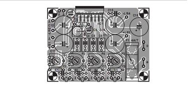


     C15 and C16 are local bypass capacitors for the supply voltage. The power supply ripple rejection of the TDA7375A is approximately 50 dB. If you want to use only a transformer, bridge rectifier and smoothing capacitor for the power supply, the minimum requirement is a transformer rated at 12 V / 30 VA in combination with a 10,000-µF electrolytic capacitor (remember that the maximum allowable supply voltage is 18 V). One of the few drawbacks of this quad amplifier is that two of the channels are inverted with respect to the other two. For this reason, the polarity of each loudspeaker terminal is marked on the circuit board layout (e.g., +LS1 and –LS4) to indicate which terminal of the loudspeaker should be connected where.


    Radial electrolytic capacitors rated at 3300µF/16V and having a diameter of only 12 mm are used for the output capacitors, which allows the circuit board to remain relatively compact. Our preferred type of electrolytic capacitor is a member of the Rubycon ZL series, which can handle no less than 3.4 A of ripple current. The maximum current consumption of the circuit with all four channels driven to the clipping level (with 4-Ω loads) is approximately 2.1 A. The TDA7375A can also be used with 2-Ω loads. However, in this case the internal temperature rises considerably, since the Multiwatt 15V package has a rather large thermal impedance of 1.8 ºC/W.
    In the interest of the service life of the IC, it is thus a good idea to use a somewhat larger heat sink. A 4 A/T fuse has been selected in consideration of possible 2-Ω operation. If you limit the load to 4 Ω, the fuse value can be reduced to 2 A/T. The output terminals of the amplifiers can be found on the circuit board next to the associated electrolytic capacitors. The related ground connections for LS1 and LS2 are located next to the LS1 and LS2 terminals, but the ground connections for LS3 and LS4 are located on the left, next to the IC, since this gives the best current paths on the circuit board and the least distortion. Vertical car connectors (spade terminals) are used for the power supply connections.
    Resistors:
    R1-R4 = 100Ω
    R5 = 10kΩ
    R6 = 0Ω1, 5W
    P1-P4 = 10 k preset
    Capacitors:
    C1,C3,C5,C7 = 15nF
    C2,C4,C6,C8 = 220nF
    C9 = 10µF 63V radial
    C10 = 47µF 25V radial
    C11-C14 = 3300µF 16V
    C15 = 100nF
    C16 = 1000µF 25V radial, max. diameter 13mm
    Semiconductors:
    IC1 = TDA7375A (ST)
    Miscellaneous:
    F1 = fuse, 4A/T (time lag), with PCB mount holder 2 fast-on (spade) terminal, male, vertical, solder type (2-pin version)
    Measurement results
    Supply voltage = 14.4 V
    Quiescent current = 100 mA
    Pmax. (0.1% THD) = 4 × 5.3 W/ 4Ω
    Input sensitivity = (5.2 W/4 Ω) 0.5 V
    THD+N (B = 80 kHz, 1 kHz 1W/4 Ω) = < 0.04 % Bandwidth = 28 Hz to 55 kHz

    100W Quad Car Amplifier circuits.
    { Read More }


    Cable TV amplifier circuits

    Description.
    This is a very simple cable TV amplifier using two transistors. This amplifier circuit is most suitable for cable TV systems using 75 Ohm coaxial cables and works fine up to 150MHz. Transistor T1 performs the job of amplification. Up to 20dB gain can be expected from the circuit.T2 is wired as an emitter follower to increase current gain.
     
     Circuit diagram


    Notes.
    • The circuit can be assembled on a Vero board.
    • Use 12V DC for powering the circuit.
    • Type no of the transistors are not very critical.
    • Any medium power NPN RF transistors can be used in place of T1 and T2.
    • This is just an elementary circuit. Do not compare it with high quality Cable TV amplifiers available in the market.
    { Read More }


    Wednesday, May 29, 2013

    STK4241V 120W stereo amplifier

    This Home Stereo Amp is equiped with STK4241V wich is a thick film hybrid IC, AF Power Amplifier (Split Power Supply) (120W+120W min, THD = 0.08%). STK4241V has some features like:
    • Muting circuit built-in to isolate all types of shock noise
    • Current mirror circuit for low 0.08% total harmonic distortion
    For this 2x120W home stereo power audio amplifier we use a single monochip STK4241V to obtain up to 120W for each channel.


    Amplifier home stereo components:
    R6, R22 – 560 ohm / 0.125W
    R1, R24 – 1K / 0.125W
    R9, R10 – 1K / 0.5W
    R7, R18 – 4.7K / 0.25W
    R8, R19 – 4.7K / 0.5K
    R2, R5, R21, R23 – 56K / 0.125W
    C7, C17 – 3pF ceramic
    C2, C20 – 470pF ceramic 50V
    C6, C16 – 1nF 100V
    C11, C12 – 100nF 100V
    C1, C19 – 2.2uF 50V
    C5, C15 – 1uF 63V
    C4, C10, C13 – 10uF 63V
    C9, C14 – 47uF 63V
    C8, C18 – 100uF 16V


    source [link] 
    { Read More }


    Balanced Microphone Amplifier

    We published a design for a stereo microphone preamplifier with balanced inputs and a phantom power supply. The heart of this circuit was a special Analog Devices IC, the SSM2017. Unfortunately, this IC has been discontinued. In its place, the company recommends using the pin-compatible AMP02 from its current product line. However, and again unfortunately, the specifications of this opamp make it considerably less suitable for use as a microphone amplifier. By contrast, Texas Instruments (in their Burr Brown product line) offer an integrated instrumentation amplifier (type 1NA217) that has better specifications for this purpose. Incidentally, this IC is also recommended as a replacement for the SSM2017. It features internal current feedback, which ensures low distortion (THD + noise is 0.004 % at a gain of 100), low input-stage noise (1.3 nV/√Hz) and wide bandwidth (800 kHz at a gain of 100). The supply voltage range is ±4.5 V to ±18 V. The maximum current consumption of the 1NA217 is ±12 mA.

    Circuit diagram :

    Balanced Microphone Amplifier Circuit Diagram

    Balanced Microphone Amplifier circuit Diagram

    The gain is determined by only one resistance, which is the resistance between pins 1 and 8 of the IC. The circuit shown here is a standard application circuit for this instrumentation amplifier. R1 and R2 provide a separate phantom supply for the microphone connected to the amplifier (this is primarily used with professional equipment). This supply can be enabled or disabled using S1. C1 and C2 prevent the phantom voltage from appearing at the inputs of the amplifier. If a phantom supply is not used, R1 and R2 can be omitted, and it is then better to use MKT types for C1 and C2. Diodes D1–D4 are included to protect the inputs of the 1NA217 against high input voltages (such as may occur when the phantom supply is switched on). R4 and R5 hold the bias voltage of the input stage at ground potential. The gain is made variable by including potentiometer P1 in series with R6. A special reverse log-taper audio potentiometer is recommended for P1 to allow the volume adjustment to follow a linear dB scale.

    The input bias currents (12 µA maximum!) produce an offset voltage across the input resistors (R4 and R5). Depending on the gain, this can lead to a rather large offset voltage at the output (several volts). If you want to avoid using a decoupling capacitor at the output, an active offset compensation circuit provides a solution. In this circuit, a FET-input opamp with a low input offset (an OPA137) is used for this purpose. It acts as an integrator that provides reverse feedback to pin 5, so the DC output level is always held to 0 V. This opamp is not in the audio signal path, so it does not affect signal quality. Naturally, other types of low-offset opamps could also be used for this purpose. The current consumption of the circuit is primarily determined by the quiescent current of IC1, since the OPA137 consumes only 0.22 mA.

    Author: T. Giesberts - Copyright: Elektor Electronics

    { Read More }


    Friday, May 17, 2013

    30W VHF FM Broadcast Amplifier

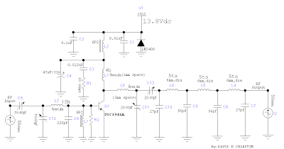
    The 30 watt amplifier circuit shown below provides an appropriate power boost with an input of 4 watt up to 6 watts. The circuit is designed to cover 88-108MHz FM Broadcast Band. However, the circuit is very stable at my place and provides a clean-output through seven (7) element Butter-worth low-pass filter.
    30W VHF FM Broadcast Amplifier
    The heart of the circuit is 2SC1946A VHF RF power transistor. The transistor is specifically designed to operate at frequencies up to 175 MHz, with very good results.

    The feedline is decoupled. The current amplifier can be more than 5 amps. All coils are made of 16gauge wire rod (copper or silver wire can do better) and HF RFC may be central torus (as shown in the image) or 6-hole ferrite R1 bead.C3 and snubber circuit forms, while R2 and C6 prevent the amplifier self-oscillation in VHF, it is sometimes necessary to add 180 ohms in parallel with the amplifier will L7.That to dispel UNDESIRABLE VHF thereby reduce the spurious level.

    The 60Watts VHF power amplifier using the above circuit. 2SC1946A Two transistors are arranged at 90 degrees to each other and their results were combined using "Network Power Combiner". It is very difficult to combine skills in the VHF and UHF

    { Read More }


    Tuesday, April 9, 2013

    Datasheet IC Amplifier AN7143 BA5406

    This time I will post about datasheet of some IC that was applied to the power amplifier. Some of his IC from IC AN7143, AN7145L, AN7145H, AN .... , Up to BA5406. Here is the datasheet it in the form of images that you can download.

    datasheet IC AN7143 sampai BA5406
    Datasheet IC Amplifier AN7143 - BA5406
    { Read More }


    Wednesday, April 3, 2013

    BTL Stereo Amplifier TDA7052 3

    This is BTL stereo power amplifier with basic amplifier on IC TDA7052 / TDA7053

    BTL Stereo Amplifier TDA7052 / 3
    { Read More }


    Monday, April 1, 2013

    Making Home Theater 5 1 Surround Amplifier

    5.1 Surround Amplifier
    Actually, 5.1 channel amplifier consists of 6 amplifiers 1 channel mono, which has certain specifications on each canals. Has 6 channel surround sound amplifier that consists of Front Left | Center | Front Right | Rear Left (Left Surround) | Rear Right (Right Surround) | and LFE (Subwoofer).


    For clarity I give a simple illustration of the layout and the circuit for these speakers.


    5.1 Speaker Setup
    5.1 Speaker Setup

    Accoustic Field Generator

    Acoustic Field Generator is generating acoustic sound with surround effects are adjustable with a standard Dolby Surround, able to produce surround sound is good enough but not too much need of funds. Technological developments as if not only focused on one area alone but on all fronts. The development of technologies that exist today one of them is in the field of audio. With more advanced audio technology today not only as mere entertainment but has become a hobby, hobby is not cheap of course. Many audio enthusiasts trying to make music sound that sounded to be very hard to make music sound as live, the addition of the amplifier, woofer or special speakers that cost is not cheap.

    The sound effects are living seems to now is something that most do not have to exist in every good audio devices. This effect is basically a surround effect that can lead to sound as though coming from different directions and his voice can still be heard clearly. Currently Compo-tape tape that has been a lot of these facilities surround sound but not good enough when heard from a considerable distance because of the effects surroundnya missing. This is because the distance is too far listener and speaker, speaker layout is not quite right, or the effect of unfavorable surround.

    Surround effects are nice and can be heard with a good surround system is a system that is in movie theaters and to make it not a bit prangkat needed funds. However, if satisfaction remains the number one then the fund is not a major problem. To find a middle ground between price and quality surround effects it was attempted to make the Acoustic Field Generator that can produce surround sound is good enough but not too much need of funds. Acoustic Field Generator is capable of generating acoustic sound with surround effects are adjustable with a standard Dolby Surround.

    Accoustic Field Generator Construction


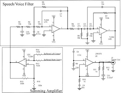
    Basically an Acoustic Field Generator built from op-amp circuit and filters. Op-amps are usually used as a voltage amplifier in the Acoustic Field Generator is more widely used as active filters. The filter in the tool is very instrumental in creating an acoustic sound that is really clear, but in practice, almost all the filters, do not miss the precision of the signal with a specific frequency. An op-amp is good for this application is the op-amp which has a wide bandwidth, rise time, slew rate and fast setting timenya. In addition to op-amp and active filter, theres more important parts of the power supply. This is the part that is instrumental in creating excellence acoustic sound because of the bad power supply which is the only producer of noise, which will enter into a voice signal path so that should clear acoustic sound into an acoustic sound with the addition of reverberation (noise). The power supply used is the twin power supply + / - 18 volts DC. Part Acoustic Field Generators

    Before we start doing this project, it helps us know in advance about the function of each speaker.

    Front Channel

    Channel Front is a forward channel input signal LR. LR signal is passed to an amplifier with gain = 1 so that this signal is passed without change / to filter the input signal LR. Front Left and Front Right, is a public speaker that we encountered in stereo amplifier, consisting of a woofer and tweeter. Woofers generally produce low tone sound with a frequency range ranging from 80Hz - 250Hz, while the tweeter produces a high tone with a frequency range between 15kHz - 20kHz. For projects that we will create, its good we use a good quality woofer, with a size of 10 inches and a type piezoelectric tweeter for each speaker fronts.

    Front Channel 5.1 Amplifier
    Front Channel 5.1 Amplifier

    Center Channel

    Center, the fullrange speakers, which produce sound with a frequency range between 80Hz - 10Khz. Output from the center speaker is a summation of left and right signal (left + right = center). In a movie or song Dolby Surround format, commonly used center for dialogue / vocal or speech of the actor / artist of a film and to produce a sound that moves ahead of us.

    Center Channel 5.1 Amplifier
    Center Channel 5.1 Amplifier


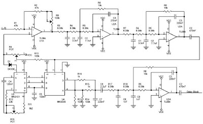
    Rear Channel with Surround System

    In this section is the core of this hard perangakat. These sections produce surround effects. To produce the surround effect is required special IC MN3005 / 8 and MN3101. Both these ICs will delay the incoming signal in several phases, so that the signal output from this phase will be left with a signal phase of the signal lain.Pada this section L and R are deducted (LR) and then passed in the buffer, filter LPF, delay line, filter LPF (7KHz) and the last is a splitter between the signals R and L. Circuit which causes the surround effect is 75KHz LPF circuit that produces its output fed to the Right Rear 75KHz LPF amplifier input while it diparalel with the Left Rear amplifier input so as to produce two signals L and R which is basically a LR signal a phase lag with the original signal phase.

    Rear Left and Rear Right, also known as surround speakers. This speaker is generally a semi-midrange speaker (usually used on television or Mini Compo), commonly called satellite speakers. In a movie surround speakers are used to generate the audible sound of distant voices or sounds that move from the back of our approach. In a music surround speakers produce sound backing vocals and generally sounds like guitars, violins and trumpets sounded clear here.

    Rear Channel 5.1 Amplifier
    Rear Channel 5.1 Amplifier

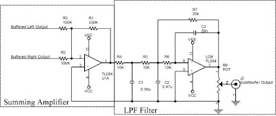
    Subwoofer Channel

    Part of this subwoofer is the summation of inputs L and R inputs to a summing amplifier. The output of the summing amplifier is passed to a class 2A LPF which will only pass signals with frequency rendah.Subwoofer, sometimes referred to as LFE (Low Frequency Effect). For these speakers using a subwoofer speaker. Speaker woofer speaker subwoofer is designed specifically to be able to respond to sound with a very low frequency, ranging from 15Hz - 120Hz. For low tone effect can be produced by either (without any harmonic frequency), then the acoustic box / box speakers are also designed specifically with a variety of methods (there are no visible speaker / inside the box, there are that use insulation / labyrinth, etc. ), so that the speaker is capable of compressing the air effectively, so that will feel the effect.

    Subwoofer Channel 5.1 Amplifier
    Subwoofer Channel 5.1 Amplifier


    Wiring Diagram Home Theater Amplifier / 5.1 Amplifier
    Wiring Diagram Home Theater Amplifier / 5.1 Amplifier

    { Read More }


    Friday, March 29, 2013

    Video Amplifier

    The video amplifier in the diagram is a well-known design. Simple, yet very useful, were it not for the ease with which the transistors can be damaged if the potentiometers (black level and signal amplitude) are in their extreme position. Fortunately, this can be obviated by the addition of two resistors. If in the diagram R3 and R4 were direct connections, as in the original design, and P1 were fully clockwise and P2 fully anticlockwise, such a large base current would flow through T1 that this transistor would give up the ghost.

    Video Amplifier Circuit DiagramMoreover, with the wiper of P2 at earth level, the base current of T2 would be dangerously high. Resistors R3 and R4 are sufficient protection against such mishaps, since they limit the base currents to a level of not more than 5mA. Shunt capacitor C4 prevents R4 having an adverse effect on the amplification.
    { Read More }


    IconIconIconFollow Me on Pinterest