Tuesday, April 30, 2013

Maximite Stepper Motor Interface

This simple circuit and program listing allows the Maximite microcomputer (SILICON CHIP, March-May 2011) to control a stepper motor. It could be expanded to allow for the control of multiple motors, with four of the Maximite’s external I/O pins used to control each motor with identical driver circuits. A ULN2003 Darlington transistor array (IC1) switches current through the stepper motor’s two windings in either direction. When one of the four Maximite output pins (8, 12, 16 & 20, corresponding to I/Os 19, 17, 15 & 13) goes high, the corresponding output pin on IC1 goes low, sinking current through a motor winding. Conversely, when these pins are high, the corresponding Darlington transistor is off and so no current flows through that portion of the winding.

Maximite stepper motor interface
The centre tap of each motor winding is connected to a current source comprising PNP Darlington transistor Q1 and some resistors. The maximum current is determined by the resistive divider driving its high-impedance base, setting the base voltage to around 9.1V when it is fully on. By adding Q1’s base-emitter voltage (1.4V at 0.5A, as per the data sheet) we can determine that there will be around 1.5V across the 3.3O resistor (12V - 10.5V), resulting in a current of 1.5V ÷ 3.3O = ~450mA. Transistor Q1 must be fitted with a medium-sized flag heatsink (Jaycar HH8504, Altronics H0637) or larger to handle its maximum dissipation of (10.5V - 4.9V) x 450mA = 2.5W.

When one of the Darlington transistors switches off and current flow through the corresponding motor winding ceases, the inductive winding generates a back-EMF current which causes the voltage across that winding to spike. IC1 has internal “free-wheeling” diodes from each output to the COM pin, which is connected to the +12V supply. The back-EMF current flows back into the power supply and the voltage spikes are clamped at about 12.7V, so that the Darlington transistors do not suffer collector reverse breakdown, which might damage them.

A 470µF capacitor provides supply bypassing for the motor while a 47kO pull-up resistor and toggle switch/pushbutton S1 drives input pin 9 of the Maximite, allowing manual control of the motor direction. Table 1 shows the sequence in which the output pins are driven to turn the motor forward; the steps are run backwards for reverse operation. The delay between the steps determines the speed at which the motor rotates. The source code of the sample program is available for download from the SILICON CHIP website (maximite_stepper_motor.bas).
{ Read More }


Sunday, April 21, 2013

Battery Equality Monitor

Almost all 24V power systems in trucks, 4WDs, RVs, boats, etc, employ two series-connected 12V lead-acid batteries. The charging system can only maintain the sum of the individual battery voltages. If one battery is failing, this circuit will light a LED. Hence impending battery problems can be forecast. The circuit works by detecting a voltage difference between the two series connected 12V batteries. Idle current is low enough to allow the unit to be permanently left across the batteries.
Circuit diagram:
battery_equality_monitor_schematic_circuit_diagramw
Parts:
R1 = 2.K
R2 = 4.7K
R3 = 39K
R4 = 39K
R5 = 1.5K
R6 = 1.5K
Q1 = BC547
Q2 = BC547
Q3 = BC557
D1 = 3mm Red LED
D2 = 3mm GreenLED
B1 = DC 12 Volt
B2 = DC 12 Volt


{ Read More }


USB Switch Schematic Circuit

Anyone experimenting or developing USB ported peripheral hardware soon be comes irritated by the need to disconnect and connect the plug  in order to reestablish communication with the PC. This process is necessary for example each time the peripheral equipment is reset or a new version of the firmware is installed. As well as tiresome it eventually leads to excessive contact wear in the USB connector. The answer is to build this electronic isolator which disconnects the peripheral device at the touch of a button. This is guaranteed to reduce any physical wear and tear and restore calm once again to the workplace. 

Circuit image :
 USB Switch-Image
USB Switch Schematic Circuit Image

The circuit uses a quad analogue switch type 74HC4066. Two of the switches in the package are used to isolate the data path. The remaining two are used in a classic bistable flip-flop configuration which is normally built using transistors. A power MOSFET switches the power supply current to the USB device.  Capacitor C2 ensures that the flip flop always  powers-up in a defined state when plugged  into the USB socket (‘B’ in the diagram). 

The  peripheral device connected to USB socket ‘A’  will therefore always be ‘not connected’ until  pushbutton S2 is pressed. This flips the bistable, turning on both analogue gates in the data lines and switching the MOSFET on. The  PC now recognises the USB device. Pressing  S1 disconnects the device.
Circuit diagram :
USB Switch-Circuit-daigram
USB Switch Schematic Circuit Diagram

The circuit does not sequence the connections as a physical USB connector does; the power supply connection strips are slightly longer than the two inner data carrying strips to ensure the peripheral receives power before the data signals are connected. The electronic switch does not suffer from the same contact problems as the physical  connector so these measures are not required in the circuit. The  simple circuit can quite easily be constructed on a small  square of perforated strip-board. 

The design uses the 74HC(T)4066 type analogue switch, these have  better characteristics compared to the standard 4066 device. The USB switch is suitable for both low-speed (1.5 MBit/ s) and full-speed (12 MBit/s) USB ports applications but the proper ties of the analogue switches and perf-board construction  will not support hi-speed (480 MBit/s) USB operation. 

The IRFD9024 MOSFET can pass a current of  up to 500 mA to the peripheral device with-out any problem.


Source : www.ecircuitslab.com
{ Read More }


Saturday, April 13, 2013

Simple Solar Tracking System

Generally, solar panels are stationary and do not follow the movement of the sun. Here is a solar tracker system that tracks the sun’s movement across the sky and tries to maintain the solar panel perpendicular to the sun’s rays, ensuring that the maximum amount of sunlight is incident on the panel throughout the day. The solar tracker starts following the sun right from dawn, throughout the day till evening, and starts all over again from the dawn next day.
Solar Tracking System
Fig. 1: Circuit of solar tracking system
Fig. 1 shows the circuit of the solar tracking system. The solar tracker comprises comparator IC LM339, H-bridge motor driver IC L293D (IC2) and a few discrete components. Light-dependent resistors LDR1 through LDR4 are used as sensors to detect the panel’s position relative to the sun. These provide the signal to motor driver IC2 to move the solar panel in the sun’s direction. LDR1 and LDR2 are fixed at the edges of the solar panel along the X axis, and connected to comparators A1 and A2, respectively. Presets VR1 and VR2 are set to get low comparator output at pins 2 and 1 of comparators A1 and A2, respectively, so as to stop motor M1 when the sun’s rays are perpendicular to the solar panel.

When LDR2 receives more light than LDR1, it offers lower resistance than LDR1, providing a high input to comparators A1 and A2 at pins 4 and 7, respectively. As a result, output pin 1 of comparator A2 goes high to rotate motor M1 in one direction (say, anti-clockwise) and turn the solar panel.

When LDR1 receives more light than LDR2, it offers lower resistance than LDR2, giving a low input to comparators A1 and A2 at pins 4 and 7, respectively. As the voltage at pin 5 of comparator A1 is now higher than the voltage at its pin 4, its output pin 2 goes high. As a result, motor M1 rotates in the opposite direction (say, clock-wise) and the solar panel turns.


Fig. 2 Proposed assembly for the solar tracking system
Similarly, LDR3 and LDR4 track the sun along Y axis. Fig. 2 shows the proposed assembly for the solar tracking system.

{ Read More }


Simple Light Sensor Alarm circuit with NE555

This circuit despatched out an alarm when its LDR sensor is uncovered to mild with the aid of solar or lamp. A 555 astable multivibrator was once used here which despatched sign a tone of about 1kHz upon detecting mild.The sensor when exposed by gentle fulls the circuit and makes the 555 oscillate at about 1kHz with transistor to power current.

The sensor can be shown within the circuit diagram. It has to positioned making an angle of about 30 – 45 stages to the bottom.

Sensitivity will also be modify with P1.  This makes the solar gentle to float thru it to the bottom and stops the alarm from happening as a outcome of the saved mild on the sensor.


{ Read More }


Cheap Bicycle Alarm Schematics Circuit

The writer needed an extraordinarily low cost and simple alarm for some of hellos possessions, one of theses hellos electrically assisted bicycle. This alarm is in accordance with a low-cost window alarm, which has a time-switch delivered to it with a 1-minute time-out. The output  pulse of the 555 substitutes the reed change in the window alarm. The 555 is brought about through a sensor mounted near the entrance  wheel, in combination with a magnet that's mounted on the spokes. This sensor and the magnet have been taken from an affordable bicycle laptop. 

Circuit diagram :

Cheap Bicycle Alarm Circuit Diagram

The entrance wheel of the bicycle is stored unlocked, so that the reed  change closes momentarily when the wheel flips. This  set offs the 555, which in turn prompts the window alarm. The circuit around the 555 takes very little present and can  be powered by means of the batteries in the window alarm.  There  is just sufficient room  left inside the enclosure of the window  alarm to mount the time-switch inside of it. 

The result is a very low-cost, compact device, with handiest a single cable going to the reed swap on the front wheel. And the noise this factor produces is solely unbelievable! After about one minute the noise stops and the alarm goes again into standby mode. The bicycle alarm should be established in an not noticeable place, this type ofs underneath the saddle, inside of a (large) entrance light, in the battery compartment, etc.
Hopefully the alarm scares any attainable thief away, or at least it makes other individuals of the common public aware that one thing isnt moderately proper. 

Caution. The installation and use of this circuit could also be subject to prison restrictions for your country, state or area.

Author : Gerard Seuren
{ Read More }


PC Power Saver

This circuit is designed to help minimise the  quiescent power consumption of PCs and  notebooks, the usage of simply our previous buddy the 555  timer and a relay as the major parts. The  circuit itself dissipates round zero.5 W in operation (that is, when the linked PC is on);  when switched off (with the relay not energised) the entire power draw is precisely zero. A prerequisite for the circuit is a PC or note e-book with a USB or PS/2 keyboard socket that  is energyed best when the PC is on. The power saver can be used to change PCs  and even whole multi-way extension leads. The unit can additionally be constructed  into  an  ordinary  mains  adaptor (which will must have an earth  pin!) because the photograph of the  creator‘s prototype shows. The  PC is plugged in to the socket  at the output of the ability saver  unit, and an extra connection  is made to the keep watch over enter of  the unit from a PS/2 (keyboard or mouse) socket or USB port. Only  the 5 V provide line of the interface is used.
 
  
PC Power Saver Image

When button S1 on the facility saver  is pressed the unit turns on, and the  monostable shaped by using the 555 timer is  brought about by means of the network composed with the aid of  R4 and C7. This drives relay RE1, whose contacts close. The connected PC isn't anyw tentatively powered up by means of the relay for a length  determined  by  P1  (approximately in the vary from 5 s to 10 s). If, all through this interval, the PC fails to indicate  that it is alive through supplying 5 V from its USB or  PS/2 connector (that is, if you don't change  it on), the monostable duration will expire, the  relay will drop out and any related device  will be energyed down. No further current will  be drawn from the provision, and, after all, it  might not be that that you may imagine to turn the PC on. When-ever you want to have to show the PC on, you must  always press the button on the ability saver  quickly earlier thanhand. 

If, however, 5 V is delivered through the PC to the  input of optocoupler IC2 earlier than the monostable occasions out (which will be the case if the  PC is changeed on all over that length), the  transistor within the optocoupler will conduct  and discharge capacitor C6. The monostable  will now stay prompted and the relay will  stay energised except the PC is changeed off  and power disappears from its USB or PS/2  interface. Then, after the monostable time  duration expires, the relay will drop out and the  power saver will disconnect itself from the primarys. There isn't any want to switch anything  else off: just shut down the gadget and the  power saver will deal with the stayder.
 
Circuit diagram :
PC Power Saver Circuit Diagram
 
It is additionally  imaginable to leave the computing device as it replaces its  tool, and the ability saver will do its job  quickly after the laptop shuts down. Power for the unit itself is obtained using a  simple provide circuit based around a miniature transformer. Alternatively, a 12 V mains  adaptor can be utilized, so lengthy as a relay with a  12 V coil voltage is used for RE1. In hellos proto-type the author used a relay with a 24 V coil  connected as proven immediately to the positive  facet of reservoir capacitor C2, the 555 being  energyed from 12 V regulated from that sup-ply using R1 and D1. A fixed resistor can of  path be used instead of P1 if desired. If the  adjustment vary of P1 isn't adequate (for  example if the PC energys up very slowly) the  monostable period may additionally be elevated via the usage of  a larger capacitor at C6.  The relay must have at the least two normally-open (or changeover) contacts rated at at  least eight A. The contact in parallel with S1 is used to provide energy to the device  itself, and the opposite contact carries  all of the current for the linked  PC  or  for  the  ex tension  lead  to  which  the  PC  and  peripherals  are  related. 

Pushbutton S1 must be rated for 230 VAC  (US: one hundred twenty VAC) operation: this is no place to  make economies. The coil current for the relay  floats thru LED D5, which must therefore  be a 20 mA sort. If a low-current LED is used,  a one hundred twenty Ω resistor may additionally be connected in parallel with it to carry the staying current.  The Fujitsu FTR-F1CL024R relay used in the  creator’s prototype has a rated coil present of  16.7 mA. Optocoupler IC2 offers isolation between  the circuit and the PC, and that is protected from  reverse polarity connection with the support of diode D4. The power saver must be constructed into an insulated enclosure and great care should be  taken to be certain that there is right kind isolation  between parts and wires carrying the  majors voltage and the other phases of the circuit. In phaseicular, the connection to the PC  and related elements (R6, C5, D4 and  IC2) must be in moderation arranged with as a minimum  a 6 mm hole between them and any section of  the circuit at majors potential.
 
Author : Wolfgang Gscheidle (Germany) - Copyright : Elektor
{ Read More }


Power up down Sequencer

Whether you’re speaking about a residence cinema  or a computer system, it’s very frequently the case  that the more than a few elements of the machine have  to be fliped on or off in a relatively explicit order,  or at least, routinely. Constructing this  sort of automation system is neatly inside the  functionality of any electronics enthusiast invaluable of the identify, however on this ‘all-digital’ age,  many of the circuits of this kind to be found  in newbie electronics magazines or web-sites use a microcontroller. Even although that  is indeed a logical solution (in  extra meanss than one!), and you  would probably even say the easiest one, it  does pose issues for all those  people who don’t (yet) have the  amenities for programming these  kinds  of  IC.  So  we  decided  to  offer you now an method that’s  very different, because it only makes use of a  simple, low cost, commonly-avail-able analogue integrated circuit,  which in fact doesn’t have to  be programmed. Our project in  reality makes use of as it’s ‘brain’ an LM3914,  a familiar IC from National Semiconductors,  usually  used  for  using  LED  VU  (volume  unit)  meters. 

Circuit diagram :

Power-up/down Sequencer Circuit Diagram

Before taking a look on the circuit  for  our  mission,  let ’s  just  remind ourselves that the IC has  one analogue enter and ten out-puts supposed for riding LEDs.  It can function in ‘point’ mode,  where the LEDs light up in flip,  from first to last, depending on  the enter voltage, but just one LED is lit at  any supplyn time. Alternatively  it will most probably function  in ‘bar’ mode (this is the mode usually used  for VU meters), and on this case, the LEDs light  up one after the other, in any such means as to create a strip of light (bar) that is longer or  shorter according to the enter voltage. This is  the mode selected for the LM3914 in the circuit described in some detail under. 

So as in an effort to control the AC energyed equipment  our  sequencer  is  meant  to manage, we're using solid-state relays — four, in our example, although which you can reduce or elevate this number, as so much as a most of ten. Since the enter instruments in solid-state relays are LEDs, they can be driven right away with the help of the LM3914 outputs, for the reason that that’s precisely what they’re designed for. As best 4 relays  are on hand, these are unfold across out-puts L2, L4, L6, and L8, however you can choose  any arrangement you prefer to go nicely with the quantity  of relays you want to have to make use of. 

Resistor R7 connected to pin 7 of the LM3914  units the current fed to the LEDs by means of the LM3914  outputs. Here, it’s been set to 20 mA, due to the fact  that's the price anticipated by the solid-state  relays chosen. The input voltage utilized to  pin 5 of the LM3914 is none instead of the  voltage present throughout capacitor C1 — and  that is the place the circuit is ingenious. When  the change is set to ‘on’, C1 charges slowly  thru R5, and the LEDs of the solid-state  relays on the outputs gentle one after another  as this voltage raises; in this approach, the gadgets  being keep watch overled are energyed up within the order you’ve chosen. To energy-down, all you have  to do is flip the change so that C1 discharges  through  R5,  and  the  LEDs  go  out  in  the  reverse order to that wherein they had been lit,  in turn energying down the devices connected to the solid-state relays. Easy, isn’t it? If you’re not pleased with the sequence velocity,  all you need do is increase or reduce the  value of R5 to be in a place to alter the pace one  manner or the different.
The circuit needs to be energyed from a volt-age of around 9 to 12 V, which doesn’t even  wish to be stabilized. A easy ‘plug-top’,  ‘wall wart’ or ‘battery eliminator’ unit will be  good, just so long as it is able to supply-ing enough current to power all the LEDs. As  the LED present is set by R7 to 20 mA per LED,  it’ll be simple for you to work out the current  required, according to the collection of solid-state relays you’re the use of. 

In our prototype the kind S216S02 relays  from Sharp have been used, primarily as a consequence of they  proved comfortably on hand via mail order. They even have the good thing about being compact,  and their switching capacity of sixteen A means  which you can dispense with a heatsink if you’re  the use of them for a computer or residence cinema  system, the place the present drawn via the vari-ous gadgets will more than likely be expected to stay under  1 A. These solid-state relays should be safe by a fuse, the score of which wants to  be chosen according to the current drawn  through the tools being powered. 

Also no longere the presence across the relay time periodinals of a VDR, sometimes called a GeMOV or  SiOV, intended to protect them from any spurious voltage spikes. You can use any sort  that ’s intended for operation on 250 VAC  with none problem. The prices of fuses F1  to F4 are after all going to rely upon the  load being secure. 

Construction of the circuit shouldn’t present any particular problem, however as the solid-state relays are connected right away to AC  power, it's very important to install it in a fully-insulated case; the case can additionally be used to  mount the energy outlet sockets keep watch overled  with the aid of the circuit. Note that sockets are female  elements.
Let’s simply finish this description with the sole  restrict imposed with the help of our circuit — but it’s  very simple to agree to, providen the intended  use. In order to remain brought about, the solid-state relays must elevate a minimal holding  present, which is 50 mA within the case of the  instruments we’ve selected. In sensible terms,  this just means that each and every of the devices powered by means of our sequencer should draw as a minimal  50 mA, or in different phrases roughly 12 VA at  230 VAC, or 25 VA at a hundred and twenty VAC.

Author :Christian Tavernier
{ Read More }


Automatic Emergency Light Circuit Diagram

This is the simple circuit of automatic emergency light. It is called dark dependent circuit. A 555 timer
IC and LDR is used for this configuration. When light fall on the LDR,
its resistance is decrease and in dark position its resistance is going
high. Using these characteristics of LDR, automatic emergency light is made.
LDR
is called Light Dependent Resistor. Its resistance is inversely
proportional to the falling light on its surface. In dark, its
resistance is approximately 7k to 10k. When light fall on its surface,
its resistance is decrease to less than 1k. In the circuit, a voltage dividerarrangement circuit is used here with LDR and 10K variable resistor.

When light fall on the surface of LDR, the resistance decrease to 1k. So the voltage of the timer pin-6 is greater than 2/3 of +Vcc. For this reason the output pin-3 goes low. The base voltage of transistor BC547 is less than 0.75 volt. The transistor is OFF state. So the light is OFF.
In dark position the LDR resistance increase is high so the voltage of the trigger pin-2 decrease to less than 1/3 of +Vcc. The output pin-3 goes high so the base voltage of the transistor BC547 is greater than 0.75 volt. The transistor is ON state. So the light is ON and it emits light.
{ Read More }


Friday, April 12, 2013

Lead Acid Battery Protector

The circuit described right here can be used to  ensure  that  a  12 V  sealed  lead  acid  (SLA)  gel battery isn’t discharged too deeply. The  predominant part of the circuit is a bistable relay,  which is pushed by using the output of an op amp. 

Circuit diagram :

Lead Acid Battery Protector Circuit Diagram
The battery voltage is first diminished by way of D1, R1,  P1 and R2, and then repeatedly compared  with a reference voltage set up with the support of diode D2.  When the battery discharges too much and  its terminal voltage drops beneath the level  set by using P1, the output of the opamp becomes  High, which causes the relay to toggle. This  in turn isolates the weight from the battery. The  battery will additionally be reconnected by manner of S1 once the  battery has been changed or recharged. 

The relay used in the prototype is a 5 V bistable type made through Omron (G6AK-234P-ST-US  5 VDC). The two windings of the relay each  have a resistance of 139 Ω (for the RAL-D 5  W-K made with the aid of Fujitsu that is 167 Ω). When the  battery voltage starts to develop into too low and  the relay is being reset the present consumption of the circuit is ready 45 mA. Shortly  after the burden has been disconnected, when the battery voltage upward throughsts above the reference  voltage once more, the reset coil will no longer be  powered and the current consumption drops  back to about 2.5 mA. 

The vary of P1 has deliberately been kept  small. With a reference voltage of 5.6 V (D2)  and a voltage drop of 0.64 V throughout D1, the circuit reacts within a voltage span of eleven.5 V and  11.8 V. This vary is clearly depending on the zener diode used and the tolerance. 

For a larger span you can use a larger value  for P1 without any problems. With the potentiometer at its mid setting the circuit switches  at about 11.6 V.
 
 
Author : Jürgen Stannieder
{ Read More }


Simple Mini Power Inverter

Even robot systems occasionally need a negative supply voltage for some purpose or other, and in this kind of application in particular there is a need for an effective circuit that does  not  make  greater demands  then  necessary in terms of current or space. If a low current 5 V supply is needed and only +5 V is available, a natural manufacturer to turn  to  is  Maxim,  and indeed in this case they do not let us down.The best known integrated  circuit made by this company is the MAX232, a level shifter for serial ports with an integrated charge pump that does not need an external inductor.

Simple Mini Power Inverter   image:
Mini Power Inverter Img

Along the same lines, although with a more stable output voltage and higher efficiency, is the MAX660. The device can ‘mirror’ any input voltage between 1.5 V and 5.5 V. With a 5 V input the output is typically –4.7 V with a load of 100 mA. Efficiency at 10 mA is around 96 % and at 100 mA is around 88 %. With an open-circuit output the IC draws a quiescent current of just 120 μA.There is little to say about the circuit itself.

Simple Mini Power Inverter Circuit diagram:
Simple Mini Power Inverter Circuit Diagram

The 0 Ω resistor on pin 1 selects the operating frequency. With R1 fitted, the circuit operates at 80 kHz; without it, at 10 kHz. The combination of L1 and C5 slightly reduces ripple on the output voltage; the choice of inductor is not as critical as it would be if it formed part of the switching circuit.Gerber files for the printed circuit board (which uses some SMD components) are available for download from the Elektor website, ref. 070279-11.zip. R1, C1 and C4 are 0603 SMDs and C3 is an SMD tantalum electrolytic capacitor. Either the MAX-660CSA or the MAX660M can be used; both come in SO8 packages. L1 is a 10 μH SMD inductor rated at 300 mA.

Source: http://www.ecircuitslab.com/2011/11/even-robot-systems-occasionally-need.html 

{ Read More }


Photo Albums Wiring Diagrams Gang Switch

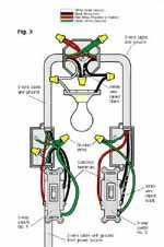
Wiring Diagram    Switch on Option 3  Fixture Between Two Three Way Switches  Power Through Switch
Option 3 Fixture Between Two Three Way Switches Power Through Switch.


Wiring Diagram    Switch on Av And Automation Industry Emagazine   Which One Should I Use  Part
Av And Automation Industry Emagazine Which One Should I Use Part.


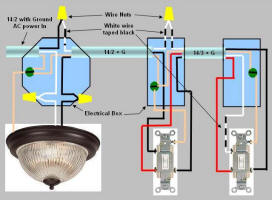
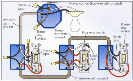
Wiring Diagram    Switch on Way Switch Wiring Diagram  Power Enters At Light Fixture Box
Way Switch Wiring Diagram Power Enters At Light Fixture Box.


Wiring Diagram    Switch on Photo Albums Wiring Diagrams Three Gang Two Way Switch
Photo Albums Wiring Diagrams Three Gang Two Way Switch.


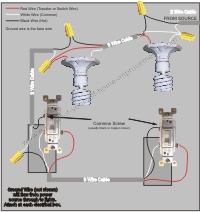
Wiring Diagram    Switch on Option  6  Power To Light    To Light    To Switch    To Switch
Option 6 Power To Light To Light To Switch To Switch.


Wiring Diagram    Switch on Way Switch Wiring    Yelp
Way Switch Wiring Yelp.


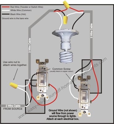
Wiring Diagram    Switch on How To Replace A 3 Way Switch  Kanderson Enterprises
How To Replace A 3 Way Switch Kanderson Enterprises.


Wiring Diagram    Switch on Normal Three Way Switches You Have Two Wiring Boxes Where The Switches
Normal Three Way Switches You Have Two Wiring Boxes Where The Switches.


Wiring Diagram    Switch on Leviton 3 Way Switch Wiring Diagram  Leviton Decora Speed Control
Leviton 3 Way Switch Wiring Diagram Leviton Decora Speed Control.


Wiring Diagram    Switch on Is Basically A 3 Way Circuit With A 4 Way Switch Added Between The 2
Is Basically A 3 Way Circuit With A 4 Way Switch Added Between The 2.


{ Read More }


Metal Detector Circuit

Metal Detector
One type of metal detector is a type of beat frequency oscillator (BFO). The methods used in metal detectors in general are changing the characteristics of the oscillator when there are close to the metal sensor. The detector works based on the resonant frequency that has been set change when there is a metal object is located quite close to the search coil sensors.


Tuning circuit (tuned circuit) should be a part of our oscillator circuit so that if approached by a metal coil sensor specific hence the output frequency of the oscillation circuit is about to change. Variation changes the output frequency depends on the frequency chosen. The selection of the higher frequency will cause the circuit sensitivity increases because the greater the frequency change. Stay if the selection frequency is too high then the practice will produce a system that is not sensitive. This is because the high frequency of most will not be reflected back but will be absorbed by the soil, building materials.

Metal Detector Circuit

Frequency used (f1-produced by the tank circuit with L1) is usually above the human hearing ability. Because it can not be heard by human pendegaran the frequency changes that occur will also not be heard as well. To overcome this it should be made a separate tone (audible frekuency-f2) which shows the change in frequency. This is said with the beat.

By mixing the two signals (f1 and f2) will produce signals f1, f2, (f1 + f2), and (f1-f2). The signal can be heard by human hearing is a signal (f1-f2). So when there are changes in frequency caused by changes in the characteristics of the search coil can be heard by humans as a rhythm-beat changing. Rhythm-beat is what is the signal (f1-f2) earlier.
VC1 setting is not easy because it requires experiments on certain metals. Similarly, for setting the rhythm of the beat is heard because at a certain condition will feel the rhythm of this beat very disturbing. So it was no possibility the beat or rhythm is not produced beatnya lower than normal because all these conditions can be set on VC1.

So when there are changes in the characteristics of the search coil it will produce sound frequency also depends on the different frequencies generated by the L1 and L2 frequencies generated by.
This method still has the disadvantage that its output frequency variation is still too small to change its frequency is almost not visible. Additionally, on certain conditions Dapa produce a frequency below the audible sound. For that we need a reconfiguration of coupling capacitors and the frequency of use.
The values ​​of existing components dirangkaian Figure 2 represents the values ​​specified in a metal. So for a specific metal component values ​​need to be adjusted especially VC1, C1, C4, and C5.

Inductor L1 is formed from the coil that serves as a search coil. This inductor will resonate along with the VC1 to produce a tank circuit with Q high. The second oscillator is formed from L2, C4, C5, R4, and Q2 and the oscillator circuit will produce a signal with a fixed frequency. D1 serves as a simple mixing between f1 and f2 and will generate a signal with a frequency (f1-f2) and a lot of harmonic signals. Signal with a frequency (f1-f2) is made so that it can be in areas that can be heard by human hearing.

Suppose that f1 and f2 on the 100KHz 101KHz then after dimixer, signal (f1-f2) will produce a signal with a frequency of 1kHz. This differential signal must be amplified in advance using a opamp that will only be able to drive headphones with high impedance. If the chill to be used for regular headphones then Dapa LM741 amplifier chip is replaced with the type of audio amplifiers. Because ampilifier audio output has a low impedance. Amplifier gain setting is determined from the setting R7 and R10, and if necessary the output of the LM741 can be incorporated into a power amplifier circuit to drive an spaker.

Circuit in Figure 2 is very simple to allow the occurrence of frequency drift - a shift in frequency. This is usually caused by the temperature factor. However this problem is not a serious problem. Permsalahan can ditanganni by searching for capacitor components which have a large enough temperature tolerance. In addition, PCB layout also has a huge effect on this problem.

The size of the search coil depends on the sensitivity of metal detectors are cooled and form of the sensor itself. For example, a large search coil which of course can easily find the metal you are looking at a large area rather than a metal detector with a small search coil. Instead of metal detectors can not determine the location of cables on a wall tertanan precisely because of the large size of the sensor.

So the greater the search coil, the accuracy of his smaller but bigger sensitivty but instead a small search coil, commonly used to compact metal detector, have high accuracy but less sensitivity. The shape of the search coil is usually a circle or square. Besides needing a shield layer which serves to reduce electrostatic effects and effects caused by capacitive objects.
{ Read More }


Home Wiring Diagram

House Wiring Diagram on Home House Wiring Installation
Home House Wiring Installation.


House Wiring Diagram on Wiring Three Way Switches The Rules Are Simple Connect The Hot Wire
Wiring Three Way Switches The Rules Are Simple Connect The Hot Wire.


House Wiring Diagram on The Figure Shows The Ring System Of Electric Wiring  Wiring Starts
The Figure Shows The Ring System Of Electric Wiring Wiring Starts.


House Wiring Diagram on Slim Films House Illustrations
Slim Films House Illustrations.


House Wiring Diagram on Home Electrical Wiring   New Home  Remodels  Additions   As You Wish
Home Electrical Wiring New Home Remodels Additions As You Wish.


House Wiring Diagram on And Then We Get To Our Homes And Offices
And Then We Get To Our Homes And Offices.


House Wiring Diagram on Home Wiring Diagram
Home Wiring Diagram.


House Wiring Diagram on Home Wiring Diagram
Home Wiring Diagram.


House Wiring Diagram on House And Home Wiring Diagram And Electrical System Png
House And Home Wiring Diagram And Electrical System Png.


House Wiring Diagram on Wiring Diagram
Wiring Diagram.


{ Read More }


Rolling Shutter Motor Control

An electrically operated rolling shutter usually has a standard control panel with a three-position switch: up, down and stop. If you would like to automate the opening and closing with a time controlled switch, a few additional wires will have to be connected. Typically, the controls are implemented as indicated in the schematic ‘Normal Situation’. If this is indeed the case, then you can see in ‘New Situation’ how the shutter can be automated with a timer. There is only one method to determine the actual schematic of your control circuit, and that is to open the control box and using an ohmmeter, pencil and paper to check out and draw the circuit. Make sure you turn the power off first though! Connect a 230-V relay (with both the contacts and the coil rated 230 VAC) to the timer.

Rolling_Shutter_Control2 Circuit Diagram 
The changeover switch between automatic and manual control needs to be rated 230 VAC as well and may not be a hazard for the user. The relay and switch are preferably fitted in a plastic mains adapter enclosure with built-in plug, which is plugged into the timer. It is a good idea to check first if this will actually fit. Because of the manual/automatic-switch, the operation is completely fail-safe and misunderstandings are out of the question. The switch prevents the issue of conflicting commands (with disastrous consequences) when, for example, the shutter is being automatically raised and manually lowered at the same time.

Rolling_Shutter_Control Circuit Diagram


Source: http://streampowers.blogspot.com/2012/06/rolling-shutter-motor-control.html
{ Read More }


Push Bike Light

Automatic switch-on when it gets dark, 6V or 3V battery operation
This design was primarily intended to allow automatic switch-on of push-bike lights when it gets dark. Obviously, it can be used for any other purpose involving one or more lamps to be switched on and off depending of light intensity. Power can be supplied by any type of battery suitable to be fitted in your bike and having a voltage in the 3 to 6 Volts range.

The Photo resistor R1 should be fitted into the box containing the complete circuit, but a hole should be made in a convenient side of the box to allow the light hitting the sensor. Trim R2 until the desired switching threshold is reached. The setup will require some experimenting, but it should not be difficult.

Push-Bike Light Circuit Diagram

Parts:
R1_____________Photo resistor (any type)
R2______________22K 1/2W Trimmer Cermet or Carbon type
R3_______________1K 1/4W Resistor
R4_______________2K7 1/4W Resistor
R5_____________330R 1/4W Resistor (See Notes)
R6_______________1R5 1W Resistor (See Notes)
D1____________1N4148 75V 150mA Diode
Q1_____________BC547 45V 200mA NPN Transistor
Q2_____________BD438 45V 4A PNP Transistor
LP1____________Filament Lamp(s) (See Notes)
SW1_____________SPST Toggle or Slider Switch
B1______________6V or 3V Battery (See Notes)

Notes:
  • In this circuit, the maximum current and voltage delivered to the lamp(s) are limited mainly by R6 (that cant be omitted if a clean and reliable switching is expected). Therefore, the Ohms Law must be used to calculate the best voltage and current values of the bulbs.
  • For example: at 6V supply, one or more 6V bulbs having a total current drawing of 500mA can be used, but for a total current drawing of 1A, 4.5V bulbs must be chosen, as the voltage drop across R6 will become 1.5V. In this case, R6 should be a 2W type.
  • At 3V supply, R6 value can be lowered to 1 or 0.5 Ohm and the operating voltage of the bulbs should be chosen accordingly, by applying the Ohms Law.
  • Example: Supply voltage = 3V, R6 = 1R, total current drawing 600mA. Choose 2.2V bulbs as the voltage drop caused by R6 will be 0.6V.
  • At 3V supply, R5 value must be changed to 100R.
  • Stand-by current is less than 500µA, provided R2 value after trimming is set at about 5K or higher: therefore, the power switch SW1 can be omitted. If R2 value is set below 5K the stand-by current will increase substantially.
Source :   http://www.ecircuitslab.com/2011/07/push-bike-light.html
{ Read More }


Portable Microphone Preamplifier

High headroom input circuitry, 9V Battery operation

This circuit is mainly intended to provide common home stereo amplifiers with a microphone input. The battery supply is a good compromise: in this manner the input circuit is free from mains low frequency hum pick-up and connection to the amplifier is more simple, due to the absence of mains cable and power supply. Using a stereo microphone the circuit must be doubled. In this case, two separate level controls are better than a dual-ganged stereo potentiometer. Low current drawing (about 2mA) ensures a long battery life.

Circuit Operation:

The circuit is based on a low noise, high gain two stage PNP and NPN transistor amplifier, using DC negative feedback through R6 to stabilize the working conditions quite precisely. Output level is attenuated by P1 but, at the same time, the stage gain is lowered due to the increased value of R5. This unusual connection of P1, helps in obtaining a high headroom input, allowing to cope with a wide range of input sources (0.2 to 200mV RMS for 1V RMS output).

Portable Microphone Preamplifier Circuit diagram:
Portable Microphone Preamplifier Circuit Diagram

Parts:
P1 = 2.2K
R1 = 100K
R2 = 100K
R3 = 100K
R4 = 8.2K
R5 = 68R
R6 = 6.8K
R7 = 1K
R8 = 1K
R9 = 150R
C1 = 1uF-63V
C2 = 100uF-25V
C3 = 100uF-25V
C4 = 100uF-25V
C5 = 22uF-25V
Q1 = BC560
Q2 = BC550

Notes:
  • Harmonic distortion is about 0.1% @ 1V RMS output (all frequencies).
  • Maximum input voltage (level control cursor set at maximum) = 25mV RMS
  • Maximum input voltage (level control cursor set at center position) = 200mV RMS
  • Enclosing the circuit in a metal case is highly recommended.
  • Simply connect the output of this device to the Aux input of your amplifier through screened cable and suitable connectors.

Source :  http://www.ecircuitslab.com/2011/06/portable-microphone-preamplifier.html
{ Read More }


Switch Mode 555 Supply

This switch-mode power supply is built around a 555 timer IC. It provides a maximum output voltage of 40 V with a 12-V input voltage. The voltage can easily be set using a Zener diode, and it must be higher than the input voltage (the minimum output voltage is always 12 V). The NE555 is used in an unconventional way here. In the normal configuration, the output of the oscillator IC is low longer than it is high. With the configuration used here, the output can be high for a shorter time than it is low. The NE555 switches FET T1 on and off.When T1 is conducting, energy is stored in L1. When T1 stops conducting, this energy is transferred to C1 and C2 via Schottky diode D1, so the voltage on these capacitors rises.

The voltage is limited by Zener diode D2.If the voltage rises above the Zener voltage,the current through the Zener diode causes T3 to conduct. This reduces the voltage on pin 5 of the NE555, which in turn decreases the relative duration of the high level on pin 3. T1 thus conducts for a shorter interval, so less energy is stored in L1 and the output voltage is stabilised.Current limiting is provided by R6, R5 and T2. If the voltage across R6 is more than 0.6 V, T2 starts to conduct. This drives T3 into conduction, causing the voltage to decrease in order to limit the current.

C5 and R7 provide a soft-start effect.The value of R1 can range from 22 kΩ for an output voltage of 15 V to 10 kΩ for an output voltage of 40 V.For the sake of safety, limit the Zener voltage to a maximum of 40 V. T1 and T2 can be rated for a maximum of 50 V. The FET is not critical; you may already have one in your spare parts bin that can switch enough current. If the coil becomes warm,the core is too small or the wire is too thin.The Schottky diode is the only component that is actually critical. Do not use an ordinary diode, since it will become much to

hot. You’re bound to find a Schottky diode in an old computer power supply (just check for a forward voltage of 0.2 V on the diode range of your multimeter).The supply shown here can deliver approximately 200 W. The input supply voltage can range from 7 V to 15 V.Don’t forget that the maximum voltage the NE555 can handle is 15 V.Finally, this power supply is not short circuit proof. A slow-blow fuse on the 12-V side is recommended.

Author : Martijn Geel Copyright :elektor elector
{ Read More }


Thread Residential Supplysingle Phase

Phase Wiring on Also  Tips On Getting Rid Of That Whinein Your Sound System
Also Tips On Getting Rid Of That Whinein Your Sound System.


Phase Wiring on Commercial Industrial Watthour Meter
Commercial Industrial Watthour Meter.


Phase Wiring on Phase Contactors Or Analog 4 20ma Input  3 Phase Contactor
Phase Contactors Or Analog 4 20ma Input 3 Phase Contactor.


Phase Wiring on Three Single Phase Transformers Sharing A Joined   Phase Wiring For  Y
Three Single Phase Transformers Sharing A Joined Phase Wiring For Y.


Phase Wiring on Cr4   Thread  3 Phase Wiring On Electrical Motor
Cr4 Thread 3 Phase Wiring On Electrical Motor.


Phase Wiring on Three Phase Wiring Plan
Three Phase Wiring Plan.


Phase Wiring on Cr4   Thread  Usa Residential Supply   Single Or Three Phase
Cr4 Thread Usa Residential Supply Single Or Three Phase.


Phase Wiring on Three Single Phase Transformers Sharing A Joined   Phase Wiring For  Y
Three Single Phase Transformers Sharing A Joined Phase Wiring For Y.


Phase Wiring on Basic Electrical Wiring   Basic Electrical Wiring Project Beginner
Basic Electrical Wiring Basic Electrical Wiring Project Beginner.


Phase Wiring on Apcscr Series Power Scr Controller User S Manual  Phase Angle
Apcscr Series Power Scr Controller User S Manual Phase Angle.


{ Read More }


IconIconIconFollow Me on Pinterest