The SCC2 is a solar charge controller, it’s function is to regulate the power flowing from a photovoltaic panel into a rechargeable battery. It features easy setup with one potentiometer for the float voltage adjustment, an equalize function for periodic overcharging, and automatic temperature compensation for better charging over a range of temperatures.
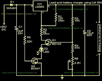
10 Amp Solar Charge Controller Circuit Diagram With Parts ListThe goal of the circuit design was to make a charge controller with analog simplicity, high efficiency, and reliability. A medium power solar system can be built with a 12V solar panel up to 10 amps, the SCC2, and a lead acid or other rechargeable up to a few hundred amp hour capacity. The SCC2 can be operated at battery voltages other than 12V, it can work at 6V and 24V by changing a few parts. Operation at voltages between 6V and 24V is also possible.
SpecificationsMaximum solar panel current: 10 Amps
Night time battery drain current: approximately 1ma
Nominal battery voltage: 6V, 12V or 24V.
TheoryThe SCC2 acts as a medium power DC current switch between the + terminals of the PV and battery. Diode D1 prevents reverse night time current flow from the battery back to the PV panel.
When the PV voltage is high enough to charge the battery, zener diode D2 conducts and turns on transistor Q2. Q2 switches the power for the rest of the circuit on. The circuit is switched off at night. IC2 provides a 5 volt regulated voltage to power the comparator circuits, it also provides a reference voltage for comparator IC1a.
When the battery voltage is below the desired full voltage and needs charging, comparator IC1a turns on and activates Q1 and Q3, this allows the solar charging current to flow into the battery. Note that Q3 is a P-channel mosfet, this allows the circuit to be wired with a common ground for the solar panel and battery. The solar current loop is drawn in heavy lines on the schematic.
When the battery reaches the full charge point, IC1a operates as a comparator based schmidt trigger oscillator, it switches the solar current off and on. The switching causes the battery voltage to oscillate a few tens of millivolts above and below the desired set point. A rail-to-rail op-amp is required for proper operation, 741 style op-amps will not work in this circuit.
The red/green charging/full LED is driven between the output of IC1a and IC1b. IC1b has an inverted version of the IC1a signal. Pin 5 of IC1b only needs an approximate center point to work as an on-off comparator, it is connected to the varying IC1a pin 2 so that it does not require another reference divider circuit.
The resistors and thermistor on the input side of IC1a form a resistive bridge circuit that is used to compare the battery voltage to a reference voltage coming from IC2/R8/R9. The potentiometer adjusts the voltage point around which the circuit will oscillate on full charge. Resistor R7 adds positive feedback to IC1a for a schmidt trigger characteristic. The thermistor provides thermal compensation, as the temperature goes down, the full voltage goes up.
The equalize switch, S1a, forces the circuit on for intentional overcharging. Switch S1b and R1 can be used to select a different float voltage range, you can experiment with this by using different values of R1, typically R1 should be greater than 1M.
Alignment Start with a charged battery, connect the solar panel directly to the
battery until the battery voltage is at or above the desired full setting,
this also that the panel is capable of charging the battery.
While measuring the battery voltage, adjust VR1 clockwise to align the
float voltage set point. If the LED turns red before it reaches the
desired float voltage, the battery will need to charge for a while.
When the battery is fully charged, it should be at the float voltage and
the led should show alternating colors.
The float voltage should be set when the board and battery are at room
temperature. Typical 12V set points are 13.8V for a gell cell and 14.5V
for a wet cell. For 6V, divide those by two, for 24V, multiply by 2.
Follow your battery manufacturers recommendations for the best settings.
Readjust the float voltage after the battery has reached a full charge.The float voltage should be set when the circuit is at room temperature.
UseConnect the solar panel to the SCC2 solar panel input connectors, connect the battery to the SCC2 output connectors. Put the solar panel in the sun, and watch the battery charge up. Systems where the battery is frequently discharged way down should occasionally be run in equalize mode for a few hours or a full day. It is best to monitor the battery voltage during this operation, disable equalization if the battery voltage goes above 16V (12V version).


 Notes
Notes