Showing posts with label schematic. Show all posts

Friday, July 12, 2013

Build LED Light Pen Schematic

Physicians and repair engineers often use small light pens for visual examination purposes. Rugged and expensive as these pens may be, their weak point is the bulb, which is a ‘serviceable’ part. In practice, that nearly always equates to ‘expensive’ and / or ‘impossible to find’ when you need one.

LEDs have a much longer life than bulbs and the latest ultra bright white ones also offer higher energy-to-light conversion efficiency. On the down side, LEDs require a small electronic helper circuit called ‘constant-current source’ to get the most out of them.
 
LED Light Pen Circuit Diagram
LED-Light-Pen-Circuit-Diagram

Here, T1 and R1 switch on the LED. R2 acts as a current sensor with T2 shunting off (most of) T1’s base bias current when the voltage developed across R2 exceeds about 0.65 V. The constant current through the white LED is calculated from

R2 = 0.65 / ILED
With some skill the complete circuit can be built such that its size is equal to an AA battery. The four button cells take the place of the other AA battery that used to be inside the light pen. Link


Author: Myo Min – Copyright: Elektor
{ Read More }


Monday, July 8, 2013

Digital Radar Speedometer Schematic

This circuit is a Digital Radar Speedometer. It allows us to evaluate the speed of any object moving, especially cars and other vehicles. The speed is calculated in kilometers per hour (KPH). Its display has three digits. This radar works with the laser reflexion. It sends laser radiation to the object and this object reflects the laser radiation to the radar. To evaluate the speed of a vehicle, we must be in front of it. In other words, the vehicle must come in our direction. The front of the radar must point the front of the vehicle. The radar has the shape of a pistol. In this radar, it has a laser LED and a laser diode. Both have a lens.

Digital Radar Speedometer Circuit Diagram


The laser LED can send a spot of light to a distance of 90 m (295 ft). Its very important that the distance range of the laser LED is 90 m, if not, the speed will not be calculated properly. The laser diode, which receives the light signal by the laser LED, must be able to detect the light which is same color as that emitted by the laser LED. The laser diode and the laser LED must be placed one beside the other. They are protected by a tinted pane. They must be placed at the front of the radar and point the outside. The radar is powered by a 9V battery and it has a SPST switch to control its power state.

The display, or the speed indicator, is placed at the rear of the radar, just on the right of the overload LED indicator. All the logic components of the circuit must be of the 74AS series and TTL type. Because they have short time of response (less than 1.7 ns) and have high frequency supports (more than 200 MHz). The radar can evaluate the speed of an object moving between 0 to 999 km/h. After this speed, the overload LED indicator will turn on and the "999" will still displayed. The radar displays the speed during 3 seconds, after this time, it displays "zero" (0).
{ Read More }


Sunday, July 7, 2013

4 5 Mhz Notch Filter Schematic

Component value sensitivity is extremely critical, as are temperature coefficients and matching of the components. Best performance is attained when perfectly matched components are used and when the gain of the amplifier is unity.

4.5 Mhz Notch Filter Schematic


To illustrate, the quality factor Q is very high as amplifier gain approaches 1 with all components matched (in fact, theoretically it approaches infinity) but decreases to about 12.5 with the amplifier gain at 0.98.
{ Read More }


Saturday, July 6, 2013

AM Receiver Schematic

This is a compact three transistor, regenerative receiver with fixed feedback. It is similar in principle to the ZN414 radio IC which is now no longer available. The design is simple and sensitivity and selectivity of the receiver are good.

AM Receiver Schematic


Notes:
All general purpose transistors should work in this circuit, I used three BC109C transistors in my prototype.The tuned circuit is designed for medium wave. I used a ferrite rod and tuning capacitor from an old radio which tuned from approximately 550 - 1600kHz. Q1 and Q2 form a compund transistor pair featuring high gain and very high input impedance. This is necessary so as not to unduly load the tank circuit.

The 120k resistor provides regenerative feedback,between Q2 output and the tank circuit input and its value affects the overall performance of the whole circuit. Too much feedback and the circuit will become unstable producing a "howling sound". Insufficient feedback and the receiver becomes "deaf". If the circuit oscillates,then R1s value may be decreased; try 68k. If there is a lack of sensitivity, then try increasing R1 to around 150k. R1 could also be replaced by a fixed resisor say 33k and a preset resistor of 100k. This will give adjustment of sensitivity and selectivity of the receiver.

Transistor Q3 has a dual purpose; it performs demodulation of the RF carrier whilst at the same time, amplifying the audio signal. Audio level varies on the strength of the received station but I had typically 10-40 mV. This will directly drive high impedance headphones or can be fed into a suitable amplifier.

Construction:
All connections should be short, a veroboard or tagstrip layout are suitable. The tuning capacitor has fixed and moving plates. The moving plates should be connected to the "cold" end of the tank circuit, this is the base of Q1, and the fixed plates to the "hot end" of the coil, the juction of R1 and C1. If connections on the capacitor are reversed, then moving your hand near the capacitor will cause unwanted stability and oscillation.

Finally here are some voltagee checks from my breadboard prototype.This should help in determining a working circuit:

All measurements made with a fresh 9volt battery and three BC109C transistors with respect to the battery negative terminal.

Q1 (b) 1.31V
Q2 (b) 0.71V
Q2 (c) 1.34V
Q3 (b) 0.62V
Q3 (c) 3.87V
{ Read More }


Wednesday, June 12, 2013

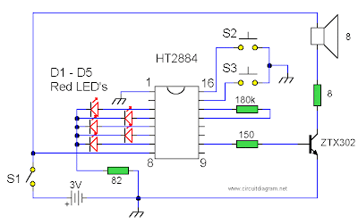
Latest Sound Effects Generator 8 different sound effects circuit schematic with explanation

Sound Effects Generator (8 different sound effects) circuit diagram

All sounds in this circuit are generated by HT2884. There are 8 different sound effect can be produced that are 2 lazer guns, 1 dual tone horn sound, 2 bomb sounds, 2 machine gun sounds and a rifle shot sound.

Note:
Power is a 3 Volt battery, but the IC will work with any voltage between 2.5 and 5 Volts. Switch S1 is the on / off switch. The output at pin 10 is amplified and drives a small 8 ohm loudspeaker. Pressing S3 once will generate all the sounds, one after another. S2 can be used to produce a single sound effect, next depression gives the next sound effect. Standby current is about 1 uA at 3 Volt, so battery life is very economical.

{ Read More }


Wednesday, June 5, 2013

Honda Civic Immobilizer System Circuit Diagramcircuit Schematic

Automotive Wiring Diagrams on Alternative Offroad Lights Or Accessory Wiring Diagram Using A Relay
Alternative Offroad Lights Or Accessory Wiring Diagram Using A Relay.


Automotive Wiring Diagrams on 1982 Jeep Cj 7 4 2 Liter Carbureted Engine Pcv System Diagram
1982 Jeep Cj 7 4 2 Liter Carbureted Engine Pcv System Diagram.


Automotive Wiring Diagrams on 1957 Ford Fairlane 500 Wiring Diagram And Electrical System Schematic
1957 Ford Fairlane 500 Wiring Diagram And Electrical System Schematic.


Automotive Wiring Diagrams on Nissan Altima Wiring Diagram And Body Electrical System Schematic
Nissan Altima Wiring Diagram And Body Electrical System Schematic.


Automotive Wiring Diagrams on The Following Schematic Shows A Typical Diagram Schematic Of Polaris
The Following Schematic Shows A Typical Diagram Schematic Of Polaris.


Automotive Wiring Diagrams on Engine Wiring Diagram 4  Automotive Wire Harness   Prestolite Wire
Engine Wiring Diagram 4 Automotive Wire Harness Prestolite Wire.


Automotive Wiring Diagrams on How One Electric Car Handles Snow  Reindeer  And Being Put Inside A
How One Electric Car Handles Snow Reindeer And Being Put Inside A.


Automotive Wiring Diagrams on Audi 80 90 Electric Mirror Wiring Diagram   Circuit Schematic
Audi 80 90 Electric Mirror Wiring Diagram Circuit Schematic.


Automotive Wiring Diagrams on Honda Civic Immobilizer System Circuit Diagram   Circuit Schematic
Honda Civic Immobilizer System Circuit Diagram Circuit Schematic.


Automotive Wiring Diagrams on Austin Metro Electric Window System Wiring Diagram   Circuit Schematic
Austin Metro Electric Window System Wiring Diagram Circuit Schematic.


{ Read More }


Sunday, June 2, 2013

Austin Metro Electric Window System Wiring Diagramcircuit Schematic

Wiring Diagram Symbols on Precision Bass Wiring Schematic   Wiring Diagram
Precision Bass Wiring Schematic Wiring Diagram.


Wiring Diagram Symbols on Diagram Electrical Wiring
Diagram Electrical Wiring.


Wiring Diagram Symbols on Floorplans With Power  Low Voltage And Structured Wiring Symbols
Floorplans With Power Low Voltage And Structured Wiring Symbols.


Wiring Diagram Symbols on Wiring Diagram
Wiring Diagram.


Wiring Diagram Symbols on Find More Information About 1996 Toyota Tercel Wiring Diagram And
Find More Information About 1996 Toyota Tercel Wiring Diagram And.


Wiring Diagram Symbols on Wiring Diagram
Wiring Diagram.


Wiring Diagram Symbols on 1987 Bmw E30 M3 Electrical Wiring Diagram Cable Harness Routing And
1987 Bmw E30 M3 Electrical Wiring Diagram Cable Harness Routing And.


Wiring Diagram Symbols on Same Symbols E G Wiring Symbols Http Hampgh Com Classmaterials Aspx
Same Symbols E G Wiring Symbols Http Hampgh Com Classmaterials Aspx.


Wiring Diagram Symbols on Austin Metro Electric Window System Wiring Diagram   Circuit Schematic
Austin Metro Electric Window System Wiring Diagram Circuit Schematic.


Wiring Diagram Symbols on Toyota Fj Cruiser Wiring Diagram And Electrical System Troubleshooting
Toyota Fj Cruiser Wiring Diagram And Electrical System Troubleshooting.


{ Read More }


Friday, May 31, 2013

Honda Civic Immobilizer System Circuit Diagramcircuit Schematic

Wire Diagram on Wiki Chevrolet Cavalier   Find Also Other Chevrolet Wiring Diagram
Wiki Chevrolet Cavalier Find Also Other Chevrolet Wiring Diagram.


Wire Diagram on Honda Civic Immobilizer System Circuit Diagram   Circuit Schematic
Honda Civic Immobilizer System Circuit Diagram Circuit Schematic.


Wire Diagram on Infiniti Wiring Diagram Wiring Harness
Infiniti Wiring Diagram Wiring Harness.


Wire Diagram on Free Wiring Diagrams   Download Free Wiring Schematics
Free Wiring Diagrams Download Free Wiring Schematics.


Wire Diagram on Wiring Diagram
Wiring Diagram.


Wire Diagram on 2002 Jeep Wrangler Tj Electrical Wiring Diagram Schematic And Pinouts
2002 Jeep Wrangler Tj Electrical Wiring Diagram Schematic And Pinouts.


Wire Diagram on Find More Info About Honda Shadow Vt1100 Wiring Diagram And
Find More Info About Honda Shadow Vt1100 Wiring Diagram And.


Wire Diagram on Honda Prelude Wiring Harness Routing And Ground Location  88
Honda Prelude Wiring Harness Routing And Ground Location 88.


Wire Diagram on 1957 Ford Fairlane 500 Wiring Diagram And Electrical System Schematic
1957 Ford Fairlane 500 Wiring Diagram And Electrical System Schematic.


Wire Diagram on Wiring Diagram   This Manual Contains Detail Explanation And
Wiring Diagram This Manual Contains Detail Explanation And.


{ Read More }


Sunday, April 21, 2013

USB Switch Schematic Circuit

Anyone experimenting or developing USB ported peripheral hardware soon be comes irritated by the need to disconnect and connect the plug  in order to reestablish communication with the PC. This process is necessary for example each time the peripheral equipment is reset or a new version of the firmware is installed. As well as tiresome it eventually leads to excessive contact wear in the USB connector. The answer is to build this electronic isolator which disconnects the peripheral device at the touch of a button. This is guaranteed to reduce any physical wear and tear and restore calm once again to the workplace. 

Circuit image :
 USB Switch-Image
USB Switch Schematic Circuit Image

The circuit uses a quad analogue switch type 74HC4066. Two of the switches in the package are used to isolate the data path. The remaining two are used in a classic bistable flip-flop configuration which is normally built using transistors. A power MOSFET switches the power supply current to the USB device.  Capacitor C2 ensures that the flip flop always  powers-up in a defined state when plugged  into the USB socket (‘B’ in the diagram). 

The  peripheral device connected to USB socket ‘A’  will therefore always be ‘not connected’ until  pushbutton S2 is pressed. This flips the bistable, turning on both analogue gates in the data lines and switching the MOSFET on. The  PC now recognises the USB device. Pressing  S1 disconnects the device.
Circuit diagram :
USB Switch-Circuit-daigram
USB Switch Schematic Circuit Diagram

The circuit does not sequence the connections as a physical USB connector does; the power supply connection strips are slightly longer than the two inner data carrying strips to ensure the peripheral receives power before the data signals are connected. The electronic switch does not suffer from the same contact problems as the physical  connector so these measures are not required in the circuit. The  simple circuit can quite easily be constructed on a small  square of perforated strip-board. 

The design uses the 74HC(T)4066 type analogue switch, these have  better characteristics compared to the standard 4066 device. The USB switch is suitable for both low-speed (1.5 MBit/ s) and full-speed (12 MBit/s) USB ports applications but the proper ties of the analogue switches and perf-board construction  will not support hi-speed (480 MBit/s) USB operation. 

The IRFD9024 MOSFET can pass a current of  up to 500 mA to the peripheral device with-out any problem.


Source : www.ecircuitslab.com
{ Read More }


IconIconIconFollow Me on Pinterest